| #series__hexo, #electronics, #project, #design | |||
Hexo - Schematic Capture, Mechanical Design, & PCB Layout |
|||
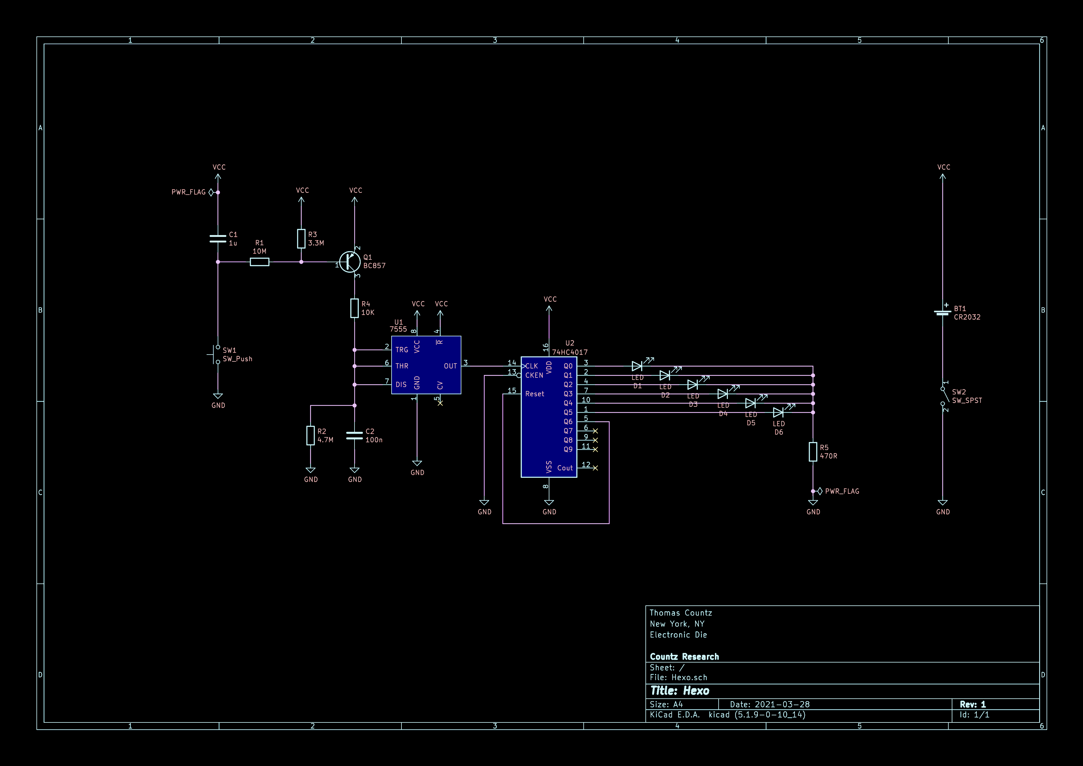
Pictured above is the schematic for Hexo’s circuit. Like I mentioned earlier, reading and interpreting a schematic is a creative process akin to jazz… although in this case it is highly precise. Not only is this a graphical representation meant to aid human designers, each component and connection is backed by a computer model which can do things like check for output pin conflicts and missed connections, in a process called electrical rules checking. I use a free open source tool called KiCAD EDA (EDA: electrical design automation) for this work.
Schematic capture is about the process of encoding a circuit into an EDA. KiCAD has a very large library of components, but also has tools for building new components, cataloging datasheets (technical document and specification produced by component manufacturers), and exporting files to use in SPICE simulations.
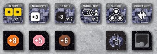
After schematic capture, I moved onto mechanical design. All I knew was that I wanted Hexo to be worn as a pendant on a necklace. In electronics projects, mechanical design is concerned primarily with the shape of the PCB as it’s often mounted without an enclosure or case. For Hexo, the PCB itself would be exposed as the final form factor and I was inspired by game pieces from one of my husband and my (mine?) favorite games, Eclipse, pictured below. Eclipse is a sci-fi based game and besides the size and shape of its pieces, I was inspired by the futuristic and mysterious vibe of the game’s design.
The mechanical design was constrained primarily by the size of the battery I planned to use (or rather the size of the mechanical clip that holds the battery) and the user experience of pressing a small button and reading the numbers. The important constraints limited how small Hexo could be because I wanted Hexo to be as small as possible (because I thought it would look cooler).
Other than that, the form factor was left to my aesthetic sense and what was feasibly manufacturable (these constraints were helpfully available on the manufacturer’s website).
I went with a 30mm x 30mm square that had three corners cut away at 45º angles because… I thought it would look cooler (sensing a theme?) and because the final surface area was within the tolerances of the manufacturer’s cheapest options. (Definitely cooler).
Finally, the PCB Layout, or the process by which you plan where to mount each component on the final board, was all that was left.
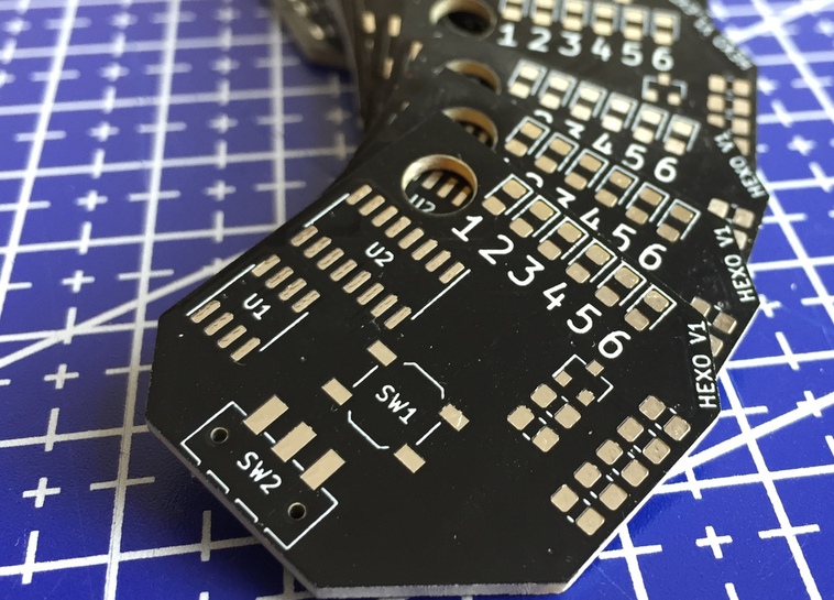
During prototyping, we used the THT (through-hole technology) components that had leads that allow them to “plug-into” a breadboard. For PCBs, we can also use SMT (surface mount technology) components that, instead of having leads that go into a hole, they have pins that are soldered to pads.
These pads are where the electrical connection between the component pins and the rest of the circuit is made. Taken together, a group of pads make up a component’s footprint or the overall shape and dimensions of the electrical connections between the component and the PCB.
In the image above, you can see the various component footprints on the bare Hexo PCBs before they were assembled.
The battery clip datasheet, pictured above, shows the only footprint I had to design by hand in CAD for Hexo (the other components used standard footprints that were pre-designed in KiCAD). The footprint is a relatively simple three square design, but it was a lot of fun to get practice at taking specs and turning them into something that would leave the page.
You can see the battery clip’s footprint as the three green squares in the layout diagram below. Note that the diagram is showing both the front and the back of Hexo at the same time and that the battery clip was mounted on the back.
![]()
The final large technical constraint, after the board shape and the component footprints, is the management of electrical traces, or the copper “wires” that run (unseen) through the board and connect everything together.
Traces are the things that connect the LED to the battery and the battery to the switch, for example. The way this is done has to do with the manufacturing process, which is step 4, so I can’t go into it here, but I will leave you this video link if you’re interested.
There’s an art to PCB layout and there are tools to help make it easier. Like a lot of design, there’s a mix of technical and aesthetic attitudes that lead to a PCB being designed one way or another. When you begin the PCB layout process, you have, what is literally called, a rats nest of traces and components that need to be untangled, taking into account electrical requirements, interference, manufacturability, etc.
Now that Hexo was designed, and (nearly) every decision that could be made, was made, it was time to send the board to the manufacturer. After which, you’ll realize that you made a tiny mistake and hope that either the manufacturer will notice and fix it, or that it was tiny enough to have no impact.